Advanced Diamond Materials & Devices for Frontier Applications
Headquartered in Hong Kong, Nova Crystal Technology Co., Ltd. is a technology-driven company dedicated to the research, development, and application of advanced diamond materials and devices. Leveraging state-of-the-art CVD and HPHT synthesis technologies, we specialize in quantum-grade, optical-grade, and thermal-grade diamond materials—delivering exceptional purity, crystallographic quality, and performance consistency.
Who We Are
Our product portfolio covers high-end diamond materials and functional devices for demanding applications including quantum sensing & computing, photonics, high-power electronics, thermal management, and precision optics. By combining advanced material growth, precision processing, and application-oriented engineering, we deliver tailored diamond solutions that meet stringent requirements of global research institutions and industrial customers.
Technology-Driven Manufacturing
Modern CVD/HPHT synthesis, controlled defect engineering, and stable batch-to-batch consistency for research-to-production transfer.
Precision Processing
Orientation control, ultra-flat polishing, edge & surface quality management, and component-level integration support.
Application Engineering
From material selection to device packaging—optimize specifications for your system constraints and performance targets.
Core Capabilities
A single partner for diamond material growth, precision processing, and functional device delivery—optimized for high-end scientific and industrial use.
What You Get
Clear specification alignment, transparent quality targets, and deliverables engineered for real integration: substrates, windows, ATR crystals, X-ray optics, thermal solutions, and customized modules.
How We Work
We start from your application constraints—optical path, wavelength/energy, thermal load, geometry, mounting—then map them to materials, tolerances, polishing grade, and packaging strategy.
Where We Create Value
Our diamond materials and devices are designed for environments where conventional materials reach performance limits.
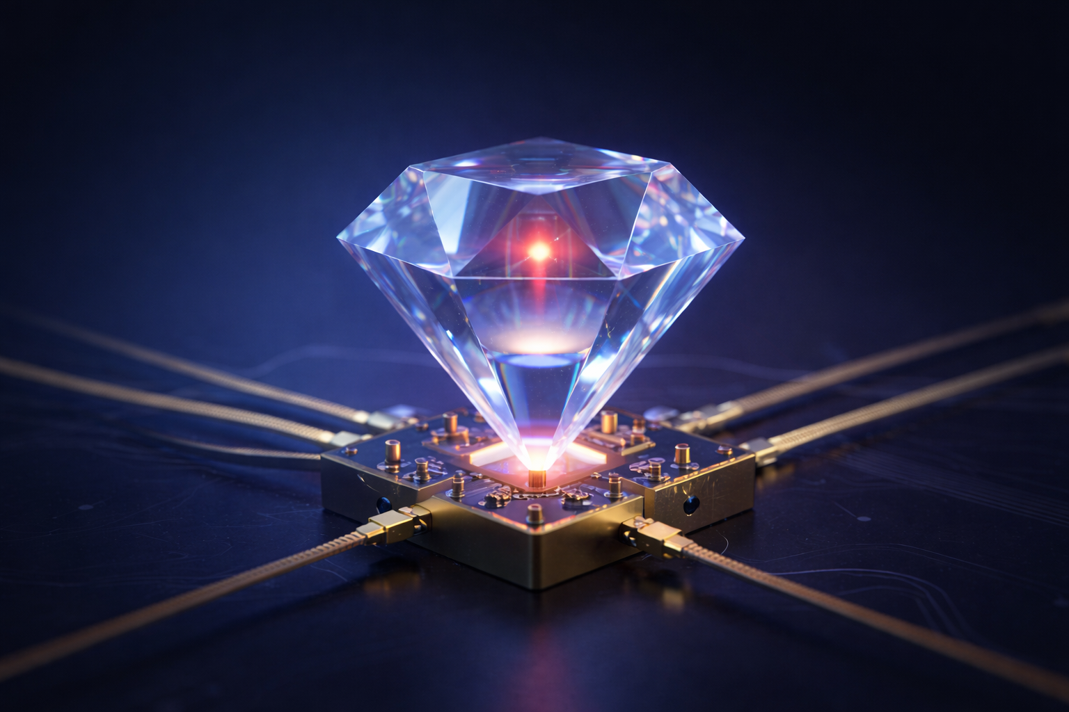
Quantum
Quantum-grade single-crystal diamond for NV/defect platforms, sensing, and quantum device prototyping.
Optics & Photonics
Optical-grade substrates, ATR crystals, and precision optical components across UV–IR (application dependent).
Thermal Management
Thermal-grade diamond wafers, diamond-copper composites, and heat spreaders for high-power systems.
Selected Collaborations & Research Ecosystem
We support global research and industrial teams with reliable diamond materials and engineering collaboration. Below are examples of institutions and large-scale platforms we frequently engage with (project-dependent).
Let’s Build Your Diamond Solution
Share your target application and constraints. We will recommend material grade, orientation, surface specification, geometry, and packaging options—then move quickly into prototyping and delivery.